All You Need To Know About PCB Assembly
The competition in industrial sector among many manufacturers and suppliers is increasing day by day. Everyone wants to gain access to more and more market while cutting their expenses and increasing profit margins. Thus growing scales of industrial automation has also created more jobs and reduced unemployment. All these things has led scientist and engineers to come up with novel ideas to make new inventions and lead the market while throwing back their competitors. In this large ocean of technology, there comes electronics industry which has high demand, very vast scope and great potential in markets and consumer devices.
The backbone of any industry indirectly related to electronics or directly electronics industry itself is the design, manufacturing and assembly of Printed Circuit Boards (PCBs). PCBs are used in almost all electronic devices, machines, equipment, instruments and other electro-mechanical machines.
In this article we will discuss about the PCBs Assembly, assembly types, assembly process, standard electronic components packages used in PCB assembly and an FAQ section to answer your basic question regarding PCB assembly.
What is PCB Assembly..?
The PCB Assembly also known as (PCBA) is the process of assembling electronic or electrical components on to the bare PCB. Assembling the components on the PCB include inserting or placement of components in designated locations on PCB and then soldering them to form electrical connections between them. There are numerous ways to handle components while assembling them on PCB. There mainly two types of components that are soldered on PCB. 1- SMT and 2- THT. SMT stands for surface mount technology and THT is Through Hole Technology.
THT Components PCBA:
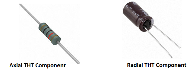
The THT components are soldered on PTH (Plated Through Hole) holes made on the PCB after fabrication process. These holes are specifically engineered to fit exactly in the lead of THT components. The PTH hole size, diameter, annular ring, copper deposition on the walls of PTH, thickness of copper and many other factors are taken care of while designing and fabricating the Through Hole PCB Board. Most of the boards used in various devices are mainly Through hole components based boards. Through holes components are mainly of two types. Radial and Axial. The radial THT component is the one that has two or both leads on one side of component. While the Axial component has one lead on one side and other lead on other side of component.
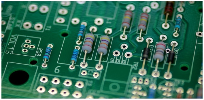
These through hole components are larger in size and takes more space on PCB. Hence the THT PCBs are not much dense.

These THT components are easy to solder and usually it is a first preference for most of hobbyist doing experiments, students doing their electronic engineering assignment/projects and professional engineers making their proof of concept prototype. A single person is enough to insert components one by one in the holes of PCB while holding the PCB board with some type of crocodile clip or vise. Then soldering with a commonly available soldering iron using lead free (preferable) solder wire.
SMT Components PCBA:
On the other hand, those components that do not have lead (Lead-less) packages of ICs, active and passive components that contain only pads (flat surfaces) for placement and soldered on PCB surface. These SMT components are available in different sizes and needs careful handling while soldering on PCB. The PCB layout designer keeps special care of dimensions of pads and vias and at PCB fabrication shop, proper PCB fabrication process of SMT based PCBs are ensured to ease the assembly process.
Surface Finish: Special finishing touch on PCB surface is given by HASL (Hot Air Solder Leveling) or ENIG (Electro-less Nickel Immersion Gold) or OSP (Organic Solder-ability Preservative). These things help increase life of PCB, reduce oxidation, helps in proper soldering and ensure stronger solder joints. The two main purpose of surface finish is to provide the solder-able surface (pads) between the SMT component and PCB surface and to protect the exposed copper circuitry.
THT Components Packages:
Dual Inline Package (DIP/PDIP):
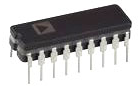
The term (DIP) stands for Dual Inline Package also known as (PDIP) Plastic DIP. This is the name of through hole (THT) package of component in which semiconductor Integrated Circuits ICs are commonly available. Most of the common micro-controllers, microprocessors, ADCs, DACs, Digital and Analog ICs are available in DIP or PDIP packages.

Ceramic DIP (CDIP):
This package is hermetically sealed in ceramic molten glass and leads are extending from both sides forming two sets of inline pins. Same as DIP and PDIP but more efficient in blocking moisture and contaminants once it is sealed.
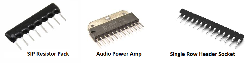
Single Inline Package (SIP):
This has a single row of pins unlike dual rows of DIP. It is commonly seen as multiple resistors with common pin, single row header sockets and audio power amplifier IC package.
SMT Components Packages:
There are lots of variants in SMT IC packages. We will discuss some of them here.
Metal electrode leadless face (MELF):
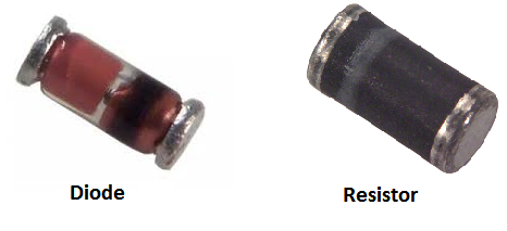
This package is commonly available in small components like resistors and diodes. The two ends are metallic and are SMT components. Special care must be taken because of their small size and roll-able shape which enable them to fall off the work bench and misplaced.
Small Outline Transistor (SOT):
The other semiconductor devices like transistor, voltage regulator, diodes, buck boost converters, switching regulators and other small package analog ICs use these SOT package of SMT components. There are different variants in SOT. SOT23 is the most commonly used. SOT23-5 means an SOT package with 5 pins. Similarly SOT23-3 means an SOT package with 3 pins. Another variant is TSOT (Thin SOT) that has a smaller height than SOT. Three types of SOT are SOT23, SOT323 and SOT416.
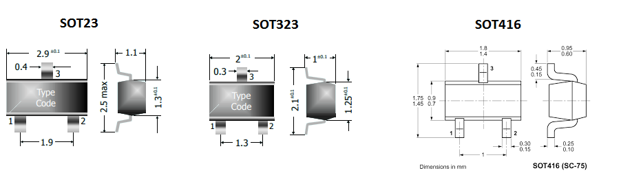
Similarly SOT23-5 and SOT353 seems similar but have different dimensions. Check out the datasheet.

Small Outline Package (SOP):
The small outline package (SOP) is widely used SMT package in ICs. It has multiple pins like 8,14 and16 pins and spacing between pins is less than 1.27mm. The SOP package falls in the category of SOIC (Small Outline IC). There are four main categories of SOIC. 1- SOP 2- SSOP 3- TSOP 4- TSSOP. The SSOP stands for Shrink SOP and lead spacing is 0.65mm. This SSOP is more compact package and smaller version of SOP.
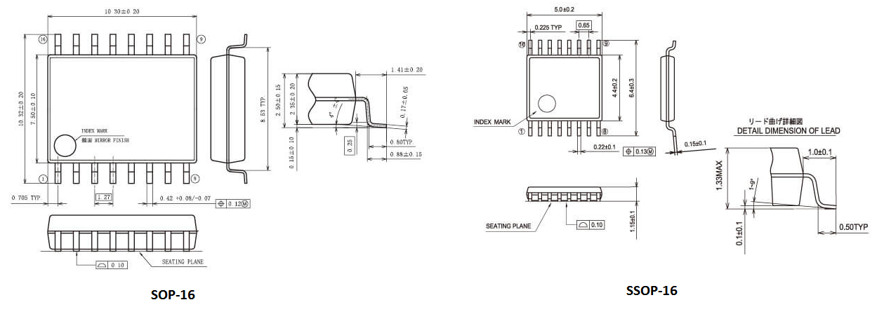
The TSOP is Thin SOP and TSSOP is Thin Shrink SOP packages. These two are also similar but little bit different in dimensions. Check out the diagram.

Quad Flat Pack (QFP):
The Quad Flat Pack (QFP) is a surface mount SMT component Integrated Circuit (IC) package. It has the “gull wing” shaped lead extending from each side of square shape IC package. The pitch range from 0.4 to 1.0mm and available in 32 to 304 pins. Other variants are LQFP and TQFP
LQFP is Low Profile QFP and TQFP is Thin QFP. TQFP has shorter leads than LQFP also the height is different L (1.4mm) and T (1.0mm). Check Diagram

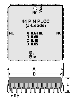
Plastic Leaded Chip Carrier:
Another most widely used type of SMT component package is “Chip Carrier”. They have the J-shaped metal leads that are turned round shaped, to make connection by solder or can be inserted in socket or can be lead-less connected on metal pads. Here the leads are not extended out of packaging like QFP. The package size is overall large to accommodate larger pin count. They are made of ceramic or plastic. They are JEDEC compliant and are available in heat-spreader and non-heat-spreader versions. The heat spreader version helps the designer to deal with less hotter version of PCB. The heat spreader is an interface between the processor PLCC package IC and the external large heat sinks to dissipate heat in air. Example of heat-spreader processor chips is shown below.
Ball Grid Array BGA:
The ball grid array (BGA) packages ICs are widely used in many high tech electronic devices. These are very difficult to handle and require special training on soldering BGA ICs. Small pitch solder balls are used along with stencil to solder the package on PCB.
