Key Techniques in Designing a Professional Multilayer PCB

The recent advancement in the field of electronics industry is the result of evolution in the PCB fabrication and PCB manufacturing techniques. The most latest and important aspect of PCB is the multiple layered PCB or multilayer PCB. In this article we will discuss about the key techniques in designing a professional multilayer PCB
The multilayer PCB is the one that has more than two copper conducting layers. It is made up of a stack of layers containing copper foil, Fiber glass prepreg and fiber glass laminate. The fiber glass prepreg epoxy resin is usually the FR-4 material commonly used in many electronic devices.
Multilayer PCB is like several double sided boards laminated together and glued to form a single thick rigid board.
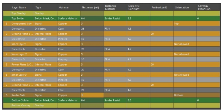
Example Multilayer PCB stack up:
The multilayer PCB has the holes, vias and pads that connect components with each other by means of copper traces. These holes are plated through holes and vias are blind and buried types. Pads are used for SMT components connection and holes are bored in PCB to connect THT components with leads.
The biggest advantage of multilayer PCB is its small size. As we know that the demand of miniature size multilayer PCB is increasing. These small form factor PCBs are now widely used in wearable electronics, small drones, in medical implant in human bodies and in small consumer electronic gadgets.
The design engineers are striving and finding ways to fit more SMT and THT components in per square inch area of multilayer PCB making them more denser, thicker and complex multilayer PCB design.
These parameters drive the design from the beginning. Like for example in high speed PCBs the designer would know that the via size may not exceed particular limit because of fabrication constraints and hence the designer would select the via size that makes the PCB fabricate and also will not compromise on the signal integrity of that particular high speed trace.
The next step is to define the layer stack-up of the multilayer PCB. This is extremely important in order to determine if the PCB is passing signal and power integrity parameters optimally. Like near end and far end cross talk between signal layers, ground bounce, electromagnetic interference and noise, signal reflection due to improper impedance matching. The arrangement of signal layers and power planes plays a crucial role in realizing a successful and working product.
Likewise, if the design includes BGA package with 1mm or lesser pitch than the number of balls on the BGA package will determine the number of signal layers in multilayer PCB. The signal fanout, routing strategy and via placement, return vias and other crucial considerations will be become significant with increasing complexity of SMT components on the board and their placement on the PCB plays a very important role in the signal and power integrity.
After the design rules are set and layer stack up is finalized, the critical nets need to be highlighted such as high speed DDR4 memory, differential pairs, USB, Ethernet, Small Form Factor Pluggable (SFP) for fiber optic, SERDES for high speed transceiver lanes in RF/digital mixed signal circuits. These nets need to be labeled correctly at the schematic stage in order to import the net list properly when design the PCB layout. Many of these signal lines will use special kind of routing tools and strategies such as line tuning, controlled impedance routing, 50 ohm and 100 ohm single ended and differential pair routing for coaxial cable and CAN bus transceivers. Altium Designer latest versions facilitates PCB designer to route a perfect trace for these signal nets with controlled length tuning while routing.
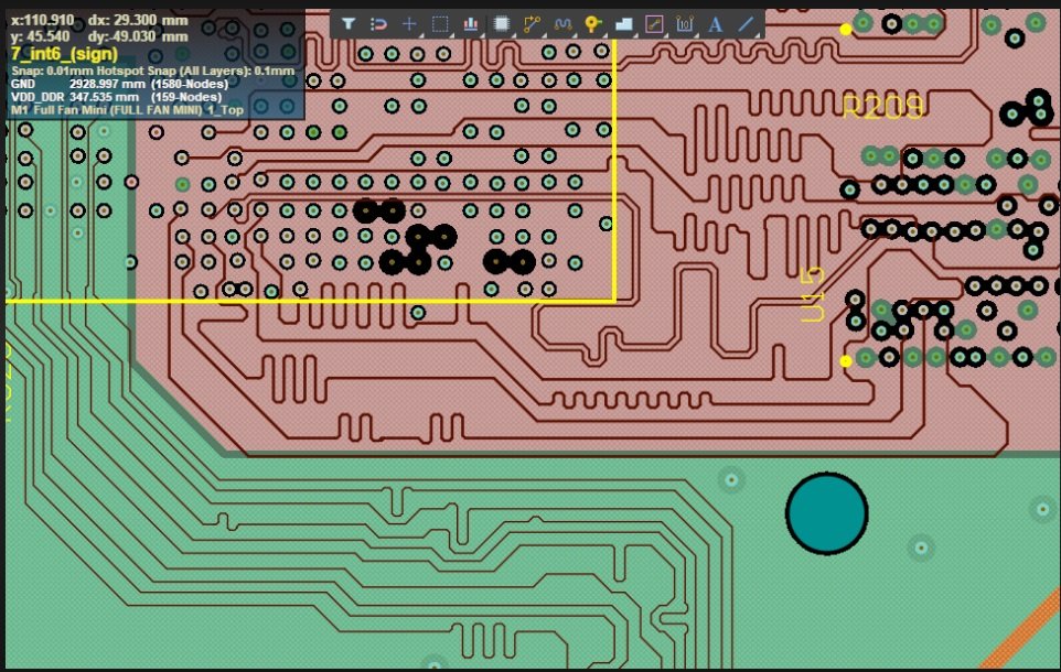
Next comes the phase of adding split planes and polygons to the design. The PCB design is nothing but the artwork. The PCB designer is an artist who is well versed with the IPC2221a standards and who knows what he or she is doing. The split planes have techniques such as avoiding planes cuts below the high speed signal traces to avoid signal discontinuity, ensuring full solid copper power plane for ground return, using thermal planes as a separate plane for dissipating heat, making the power planes such that to ensure EMC/EMI compatibility, and to ensure power integrity as per standards and use simulation software such as HyperLynx from Siemens to run SI/PI analysis.
Some of the tips and tricks of designing a professional multilayer PCB are mentioned below
- Using decoupling capacitors for power supply noise suppression near the chip,
- Keeping the traces as short and as straight as possible,
- Avoiding vias on high speed interconnects as much as possible,
- Avoid ground loops,
- Using polygon pours on top or bottom layers where necessary for power supply runs to avoid additional power plane in the stack-up to cut manufacturing cost,
- Avoiding stubs in high speed digital traces,
- Back drilling the vias on critical high speed nets,
- Keeping enough clearance between aggressor and victim traces,
- Avoiding acute angles,
- Avoiding 90 degree turns in digital traces,
- Minimizing coupling between two high speed traces,
- Ensuring to avoid component collision by incorporating mechanical 3D step models in component libraries,
- Prefer surface finish as ENIG,
- Tenting vias,
- Green solder mask,
- Using clear and bigger overlays,
- Avoiding overlays on components pads,
- Using gold fingers in PCI express connector,
- Using shielding vias throughout the RF trace,
- Stitching vias usage on the PCB top to bottom layers connected to ground net,
- Minimizing inductive loops,
- Using wider traces for high current circuits,
- 1 oz copper thickness for power circuits,
- Using via-in-pad technique if budget permits and if fabricator agrees for optimal performance,
- Using thermal vis in power devices thermal pads for heat dissipation.
Placement of components on the board play a highly significant role in the professional PCB layout design. The optimal placement with respect to ease of routing, SI/PI considerations, assembly aspect, and fitting inside the final mechanical assembly/enclosure plays 90% of the PCB design work. A cunning PCB designer will intelligently place the components on the PCB in such a way to minimize the efforts of routing signals, thus reducing the design time to less than 50%. A beautiful looking and excellent routing is impossible without strategic component placement onboard. Components of same class can be grouped together and can be copied multiple times in the PCB if the circuit is repeated many times such as 8 channel or 16 channel multiplexer or ADC/DAC circuit etc..
It is the responsibility of the PCB designer to check each and every component footprint library against the datasheet either it is 0201 package resistor or capacitor or it is a BGA, QFN, TSSOP, or any other package, either it is FMC HPC, D-Sub, terminal block connector. Any discrepancy in the actual footprint and design may lead to assembly/soldering issues later on. The PCB layout should be done in such a way to facilitate the PCB assembly team so they know which component to mount where. The Bill of Materials (BoM) designators should be printed aside the component on the PCB and those components which are not supposed to be mounted should be marked Do Not Place (DNP) on board.
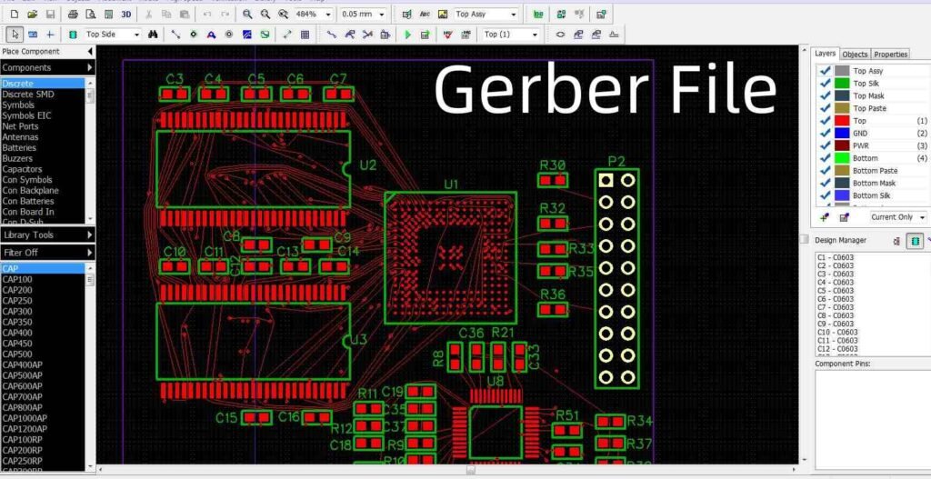
The final step if the generation of Gerber Files and assembly files for Design For Manufacturing (DFM) and Design For Assembly (DFA). These Gerber Files are the final output files in the binary format which can be fed to the plotter machine to make the negative and positive films of the PCB signal layers and power planes so they can be laminated and stacked up into a final PCB. Alongside the Numeric Controlled (NC) Drill files are generated which tells the computer about the location of plated through holes and non-plated holes in the PCB. Modern Chinese PCB manufacturers such as JLCPCB and PCBWay have online platform where the designer can simply upload the Gerber and NC Drill Files along the BoM to see the image of the PCB and get the quotation of production and assembly. This method of online submission of Gerber data in ZIP format has made the process extremely easy get the multilayer PCB fabricated, assembled, tested and shipped in no time at all. Moreover the production cost is also very cheap and the mass production or bulk production will reduce the cost per pcs further.
As PCBs have advanced, the design techniques has evolved accordingly. So much so that designing complex computing PCBs of today manually on paper seems impossible. To design a modern PCB successfully, specific electrical rules need to be followed (for each layer) to yield a durable product with stable operation throughout its lifecycle. Aside from the electrical rules, there are numerous manufacturing (physical) rules that must be followed as well for a problem-free production with high success rate. Altium Designer provides the user with the option to view their board with all of the installed components in 3D. Which makes mechanical design of your product even easier.